High frequency power amplifier um 83.1 circuit. High-frequency amplifiers on microcircuits. Arrangement of elements on the circuit board
A simple amplifier with just one transistor can be made to amplify a weak RF signal for a radio, TV or radio station.
The article below presents two diagrams simple amplifiers. H I buy it in a store, it’s cheaper to assemble an amplifier yourself, with characteristics sometimes no worse than store-bought ones.
Only a few parts are needed to assemble it. Even a novice radio amateur can handle assembling the amplifier. There are no inductors in it, the amplifiers are broadband and cover the entire range of the amplified signal, including UHF. In any case, the result was more than I expected. Most VHF local television and radio broadcasts have begun to be received with better quality, and the picture has become clearer.
Amplifier circuit diagram

The main part of this diagram high frequency transistor reverse conduction (n-p-n) Q1 (2SC2570), a circuit specially designed to amplify the VHF signal without an inductor.
If you plan to use the amplifier constantly, then you can exclude S2, which is needed to bypass the amplifier.
The amplifier is assembled on a circuit board.
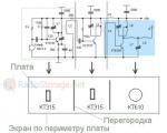
Circuit board

Arrangement of elements on the circuit board

The second version of the circuit with an additional amplifier for the HF range
Schematic diagram of a dual-band HF/VHF amplifier

In this circuit, an HF field-effect transistor amplifier is added (Q1 MFE201 N-channel two-gate and Q2 (and 2SC2570 n-p-n RF silicon transistor), which provide two independent amplifiers switched by switch S1. It turns out simple active antenna, designed to amplify signals from 3 to 3000 MHz (three ranges: 3-30 MHz high-frequency (HF) signals; 3-300 MHz very high-frequency (VHF) signals; 300-3000 MHz ultra-high frequency (UHF) signals.
Current consumption - 46 mA. The bias voltage V bjas determines the output power level (gain) of the amplifier

Fig. 33.11. Internal structure and pinout of TSH690, TSH691 microcircuits

Rice. 33.12. Typical inclusion of TSH690, TSH691 microcircuits as an amplifier in the frequency band 300-7000 MHz
and can be adjusted within 0-5.5 (6.0) V. The transmission coefficient of the TSH690 (TSH691) microcircuit at a bias voltage V bias = 2.7 V and a load resistance of 50 Ohms in a frequency band up to 450 MHz is 23 (43) dB, up to 900(950) MHz - 17(23) dB.
Practical inclusion of TSH690, TSH691 microcircuits is shown in Fig. 33.12. Recommended element values: C1=C5=100-1000 pF; C2=C4=1000 pF; C3=0.01 µF; L1 150 nH; L2 56 nH for frequencies not exceeding 450 MHz and 10 nH for frequencies up to 900 MHz. Resistor R1 can be used to regulate the output power level (can be used for a system automatic adjustment output power).
The broadband INA50311 (Fig. 33.13), manufactured by Hewlett Packard, is intended for use in mobile communications equipment, as well as in household electronic equipment, for example, as antenna amplifier or radio frequency amplifier. The operating range of the amplifier is 50-2500 MHz. Supply voltage - 5 V with current consumption up to 17 mA. Average gain

Rice. 33.13. internal structure microcircuits ΙΝΑ50311
10 dB. The maximum signal power supplied to the input at a frequency of 900 MHz is no more than 10 mW. Noise figure 3.4 dB.
A typical connection of the ΙΝΑ50311 microcircuit when powered by a 78LO05 voltage stabilizer is shown in Fig. 33.14.

Rice. 33.14. broadband amplifier on the INA50311 chip
Shustov M. A., Circuitry. 500 devices on analog chips. - St. Petersburg: Science and Technology, 2013. -352 p.
The main area of application is as part of vacuum processing equipment to ensure stable and controlled processes for applying functional coatings, plasma cleaning and etching in vacuum deposition systems.
HF GENERATOR “IVE-171RFS”
The RF (RF) generator "IVE-171RFS" is single-channel - it has an output high-frequency voltage with a frequency of 13.56 MHz and is designed to supply its active load with a resistance of 50 Ohms or to a "capacitive high-impedance load" when working in conjunction with an automatic matching device "ASU- 171S". The RF generator has a galvanically opto-isolated interface external control"RS-485", oriented for operation as part of automated equipment.
BASIC TECHNICAL DATA
Output active RF (RF) power, adjustable*, W.....from 30 to 600
Output amplitude RF (RF) voltage, adjustable*, V.....from 10 to 250
Instability of output RF (RF) power, %, no more.....3
Instability of output RF (RF) voltage, %, no more.....2
Output voltage frequency, MHz.....13.56
Maximum amplitude voltage of RF protection, V.....280
Maximum peak current of RF arc protection, A.....6
Limit of output reactive amplitude RF power, VA.....1680
Efficiency (RDC/RAS // RHF/RDC // RHF/RAS), not less than.....0.85//0.55//0.467
Electrical power consumption, W.....1300
Supply voltage.....220V -15% +10%, 48~62 Hz
Weight, kg.....15
Overall dimensions, mm.....224 x 133 x 417
* on a resistive equivalent load with a resistance of 50 Ohms via cable IVE4.171.030
The HF generator “IVE-171RFS” is a secondary power supply with a transformerless network input, operating at conversion frequencies of 45¸55 kHz and 13.56 MHz. The block is based on two assemblies of transistor converter modules, powered by: the first - variable mains voltage from single-phase noise suppression surge protector, the second - by constant adjustable power intra-block voltage received from the first module. Both are controlled via a control and signal interface module. Thus, the conversion of the mains supply voltage into a high-frequency output voltage is carried out sequentially in two stages using two modules: the first converter module and the second high-frequency power amplifier module. From the output controlled DC voltage 0V÷+60V of the first low-voltage converter module, with a power of 1.2 kW, the high-frequency power amplifier module is powered. Its output RF voltage with an amplitude of 0V÷280V and a reactive power of up to 1680VA is supplied to the output connector of the RF generator. To consume almost sinusoidal current from the supply network, the converter module circuitry and functionally performs power factor correction. The formation of all operating algorithms, processing and generation of control signals of data signals is carried out in the control and signal interface module. RF voltage with a frequency of 13.56 MHz is generated in a high-frequency power amplifier module, which includes a quartz master oscillator. Then it goes to the RF pre-amplifier, and then to the final RF power amplifier, located in the same module. From the output of the final RF power amplifier, the RF voltage is supplied to the input of the “RF measurement” unit, also located in the high-frequency power amplifier module, and from its output to the output connector of the unit. The high-frequency power amplifier module, when operating on a nominal resistive load of 50 Ohms, provides a maximum of 600 W of active power.
In addition, the high-frequency power amplifier module has a thermal protection unit that turns off the RF voltage when the power RF transistors or protective-limiting circuits overheat due to operation at unmatched modes (loads) or when operating at an ambient temperature of more than +35°C. The signals of the output RF voltage, RF current and active RF power of the RF generator, converted in type and level in the “RF measurement” unit, are sent for further processing to the control and signal interface module and to the RF protection unit. The RF protection unit calculates the reactive output RF power, the ratio of active to reactive RF power and generates signals to prohibit the operation of the final RF power amplifier when the specified levels of the output amplitude RF voltage and RF current are exceeded, thereby ensuring its protection. The RF generator has a 3.5-digit digital indication of output and set parameters: power, voltage, current, and their regulation from the front panel of the unit, as well as LED indication of all operating modes and, accordingly, their selection using buttons located on the front panel block. These indication and control elements constructively form an indication and control module. The RF generator is equipped with a fan control unit, which maintains constant thermal conditions of the converter module and high-frequency power amplifier module and increases the fan's operating life. The RF generator contains standby and service power supply modules that respectively generate standby voltage ±5V, which is necessary for the operation of the mains filter and the control and signal interface module, and service voltage +24V, which is necessary to power the fan control unit and the high-frequency power amplifier module.
The output impedance of the high-frequency power amplifier module is matched with the load impedance by the automatic matching device "ASU-171S", capable of operating in both automatic matching mode and manual control from the manual control panel.
It is possible to develop and manufacture a high-frequency generator with different output characteristics according to your technical specifications.
AUTOMATIC MATCHING DEVICE “ASU-171S”
The automatic matching device "ASU-171S" is a T-shaped "CCL-circuit" tunable by means of two variable vacuum RF capacitors, which allows you to match the load impedance with the output impedance of the RF generator. The RF RF voltage coming from the generator to the “RF INPUT” connector, passing through the “RF signal” meter installed in the ACS, enters the matching “CCL circuit” and, converted in level, is output to the output coaxial connection “RF OUT”. It also receives, after passing through the mixer assembly, a constant voltage supplied to the “DC INPUT” input connector. maximum value which should not exceed 1000V, and its current should not exceed 2A. Variable capacitors have an electric drive controlled by a control and interface module, which, based on the operating algorithm embedded in it and, receiving signals about the values of the amplitude RF voltage, RF current and active RF power from the RF signal meter, generates commands for the electric drive such in such a way that the load impedance “reduced” to the ACS input approaches 50 Ohms, and the doubled value of the ratio of effective active RF power to reactive RF power tends to unity.
The control and interface module, in addition to generating power control signals for the electric drive of variable RF capacitors, provides amplification and conversion of signals about the magnitudes of amplitude RF voltage, RF current and active RF power from the RF signal meter. Having processed them, it outputs the ratios of amplitude RF voltage to RF current and effective active RF power to reactive RF power in analog form to the “CONTROL” connector and in the form of a serial digital code to the “RS-485” connector of the external control interface. In addition, the control and interface module provides conversion and interface of control signals and ACS modes from the RS-485 interface and the manual control panel, as well as the conversion of the mains supply voltage into ±24V DC voltage to power the electric drive of variable RF capacitors.
Power amplifier 10 W
The amplifier is designed to work with a transver having a P output of up to 1 watt. The exciter load, which ensures stable operation on all ranges, is resistor R1. The setting consists of setting the quiescent current VT2 within 0.3 A (in the absence of a signal at the input).
A 1 volt signal at the input increases the output power in the antenna to 10 watts. Reception-transmission switching is carried out from an external control circuit, which is closed to the housing when switching to transmission. In this case, relay K1 is activated and connects the antenna to the output of the power amplifier. When the control circuit breaks, a positive voltage appears at the base of VT1, opening it. Accordingly, the VT1 collector is near zero. Transistor VT2 closes. Relay type RPV2/7 passport RS4.521.952 Chokes L1 and L2 type D1 (1A) with inductance 30 and 10 μH, respectively.
Frame diameter L3- 15 mm PEV2 wire 1.5 mm
Wideband power amplifier
Drozdov VV (RA3AO) To work in conjunction with an all-band HF transceiver, you can use a wideband power amplifier, circuit diagram
The amplifier is assembled using a push-pull circuit using powerful field-effect transistors VT1, VT2. The long line type transformer T1 provides the transition from an asymmetrical excitation source to the symmetrical input of a push-pull stage. Resistors R3, R4 allow you to match the input impedance of the cascade with a 50-ohm coaxial line with an SWR of no more than 1.5 in the range of 1.8 -30 MHz. Their low resistance provides the amplifier with very good resistance to self-excitation. To set the initial bias corresponding to the operation of the transistors in mode B, use the circuit Rl, R2, R5.
Diodes VD1, VD2 and VD3, VD4 together with capacitor C7 form a peak detector of the ALC circuit and protect transistors from overvoltages in the drain circuit. The operating threshold of this circuit is determined mainly by the stabilization voltage of the zener diode VD9 and is close to 98 V. Diodes VD5-VD8 serve for “instant” protection of the drain circuit from overvoltages. The T3 long line type transformer provides the transition from the amplifier's symmetrical output to an unbalanced load. To ease the requirements for the broadband of this transformer and reduce possible voltage surges in the drain circuit, a symmetrical low-pass filter C8L1C10, C9L2C11 with a cutoff frequency of about 30 MHz is connected in front of the transformer. Installation of a mounted amplifier. The amplifier is assembled on a ribbed heat sink made of duralumin with dimensions of 110x90x45 mm. The fins are milled on both sides of the radiator, their number is 2x13, the thickness of each is 2 mm, the height is 15 mm on the side of the transistor installation and 20 mm on the side of the nuts for their fastening. On the longitudinal axis of the radiator, at a distance of 25 mm from the transverse axis, areas with a diameter of 30 mm are milled for installing transistors, and with- for fastening nuts. Between the transistors, a “common wire” bus is laid on the radiator fins, cut from sheet copper 0.5 mm thick and attached to the base of the radiator with two M3 screws, passed between the two central ribs at distances of 10 mm from its edges. Tire dimensions - 90x40 mm. Mounting posts are attached to the bus. Coils L1 and L2 are frameless and wound with bare copper wire with a diameter of 1.5 mm on a mandrel with a diameter of 8 mm. With a winding length of 16 mm, they have five turns. Transformer T1 is wound with two twisted wires PEL.SHO 0.31 with a twist pitch of about three twists per centimeter on a ring magnetic core made of M400NN ferrite of standard size K10x6x5 and contains 2x9 turns. Transformers T2 and T3 are wound on ring magnetic cores made of ferrite of the same brand, standard size K32x20x6. Transformer T2 contains 2x5 turns of twisting from PELSHO 0.8 wires with a step of two twists per centimeter, T3 - 2x8 turns of such twisting. Capacitors Cl - C3 - type KM5 or KM6, C4-C7-KM4, C8-C11-KT3.
Setting up a properly assembled amplifier with serviceable parts comes down to adjusting the inductances of coils L1 and L2 for maximum output in the 30 MHz range by compressing or stretching the turns of the coils and setting the initial bias using resistor R1 to minimize intermodulation distortion in single-sideband signal amplification mode.
It should be noted that the level of distortion and harmonics largely depends on the accuracy of the selection of transistors. If it is not possible to select transistors with similar parameters, then for each transistor you should make separate circuits for setting the initial bias, and also, to minimize harmonics, select one of the resistors R3 or R4 by connecting additional ones in parallel with it.
In linear amplification mode in the ranges of 14-28 MHz, thanks to the presence of low-pass filters C8L1C10, C9L2C11, the harmonic level at the amplifier output does not exceed the permissible limit of 50 mW, and it can be connected directly to the antenna. In the ranges of 1.8-10 MHz, the amplifier should be connected to the antenna through a simple low-pass filter, similar to the C8L1C10 circuit, and two filters are sufficient, one for the ranges of 1.8 and 3.5 MHz, the other for the ranges of 7 and 10 MHz. The capacity of both capacitors of the first filter is 2200 pF, the second is 820 pF, the inductance of the coil of the first is about 1.7 μH, the second is about 0.6 μH. It is convenient to make frameless coils from bare copper wire with a diameter of 1.5 - 2 mm, wound on a mandrel with a diameter of 20 mm (the diameter of the coils is about 25 mm). The first filter coil contains 11 turns with a winding length of 30 mm, the second - six turns with a winding length of 25 mm. The filters are adjusted by stretching and compressing the turns of the coils to achieve maximum output in the ranges of 3.5 and 10 MHz. If the amplifier is used in overvoltage mode, separate filters should be turned on on each range.
The amplifier input can also be matched with a 75-ohm coaxial line. To do this, the values of resistors R3, R4 are 39 Ohms.
The power consumed from the exciter will decrease by 1.3 times, but the gain cutoff in high-frequency ranges may increase. To equalize the frequency response, coils with an experimentally selected inductance, which should be about 0.1-0.2 μH, can be connected in series with capacitors C1 and C2.
The amplifier can be directly loaded into a resistance of 75 Ohms. Thanks to the action of the ALC loop, the linear undervoltage mode of its operation will remain, but the output power will decrease by 1.5 times.
Power amplifier on KP904
E. Ivanov (RA3PAO) When repeating the UY5DJ power amplifier (1), it turned out that the most critical component that reduces the reliability of the entire amplifier is the output stage. After experiments on various types bipolar transistors
I had to go to the field. The output stage of the UT5TA broadband amplifier (2) was taken as the basis. The diagram is shown in Fig. 1. new details are highlighted with thicker lines. A small number of parts made it possible to mount the cascade on printed circuit board